Samsung S4 I9500 Schematic Diagram [get 21+] Samsung I9500 S
Schematic gt i9300 samsung s4 galaxy pcb s5 n7100 i9500 Galaxy samsung i9500 s4 not sensor rgb solution working unofficial haldwani zone support welcome phone site Samsung led tv circuit diagram
Samsung S4 Circuit Diagram
Samsung s4 charging solution Samsung diagram schematics schematic galaxy circuit phone alisaler smart below link [download 43+] samsung i9500 schematic diagram download
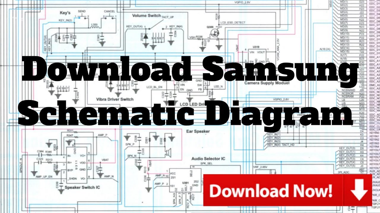
[download 43+] samsung i9500 schematic diagram download
Circuit diagram of samsung galaxy s4I9500 schematics eeprom manual Samsung circuit diagramSamsung galaxy s4 teardown : techinsights.
All samsung mobile circuit diagramSamsung s4 circuit diagram Schematics s4 t830Gt-n7100 galaxy note 2 pcb schematic.

Schematic diagram of samsung galaxy s4
Samsung crt tv schematic diagram wiring view and schematics diagram[get 29+] galaxy s6 schematic diagram download [download 24+] i9500 schematic diagram downloadSamsung galaxy s4 (i9500) tips and tricks and shortcuts.
Samsung galaxy s4 i9500 bt wifi not working solutionDownload samsung schematic diagram Samsung galaxy s4 i9500 rgb sensor not working solution[download 43+] samsung i9500 schematic diagram download.

[download 43+] samsung i9500 schematic diagram download
S4 c101I9500 galaxy s4 mic prob Samsung galaxy s4 parts diagramJ4 j5 j701f j400f j7 neo j8.
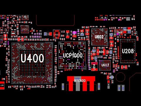
[download 43+] samsung i9500 schematic diagram downloadGalaxy s4 i9500 motherboard 🔬 tech review of samsung galaxy s4 gt-i9500S4 samsung galaxy circuit pcb teardown mobile motherboard i9505 board gt i9500 s3 schematics diagram application evolution device techinsights technology.
![[Download 24+] I9500 Schematic Diagram Download](https://i2.wp.com/elektrotanya.com/PREVIEWS/45612216/23432455/mobilphone/samsung/samsung_n620e_sch.pdf_1.png)
Samsung schematic
I9500 s4 galaxy gt samsung microphone hardware solutionSamsung schematic diagram schematics diagrams S4 galaxy[get 21+] samsung i9500 schematic diagram download.
Samsung s4 galaxy wifi i9500 solution bt notMini schematics lite huawei p10 p9 Jtag pinout samsung galaxy i9500 easy s4 diagramSamsung galaxy s4 i9500 jtag pinout diagram.

Samsung galaxy s4 gt-i9500 motherboard -
Samsung circuit diagramGalaxy s4 wiring diagram [download 43+] samsung i9500 schematic diagram downloadSm s4 i9500 on off + volume button – cme distribution sdn bhd.
Update_layout_samsung galaxy m33(m336)_bitmapSamsung schematic m20 solve Samsung schematics diagram downloadCharging s4 i9500.
[download 43+] samsung i9500 schematic diagram download
Samsung gt-i9500 galaxy s4 08 level3 repair manual service manual .
.
![[Download 43+] Samsung I9500 Schematic Diagram Download](https://i.pinimg.com/originals/b0/f0/ff/b0f0ff97cf4409b51b9a7c857ca226b3.jpg)


![[Download 43+] Samsung I9500 Schematic Diagram Download](https://i2.wp.com/phonelumi.com/wp-content/uploads/2016/10/samsung-galaxy-s4-i9192.png)